A planned Texas fab that would fold logic, memory, packaging, and test under one roof is an announced first phase — not a built plant — but the architectural ambition underneath the hyperbole is the most aggressive supply-stack bet in the chip industry’s modern history.
Fox Business and TechCrunch reported this week that SpaceX and Tesla have announced a jointly developed semiconductor facility in Grimes County, Texas, named Terafab. The project has received local approval. It has not broken ground. Those two facts are the necessary starting point for anything that follows.
The stated ambition: a building exceeding 100 million square feet — which Elon Musk described on X as “the largest and most valuable building on Earth by far” — vertically integrated to manufacture advanced logic chips, produce memory, and handle packaging and test, all under one roof. Target customers are internal: processors for Tesla’s Optimus robots and Cybercabs, and high-power chips for SpaceX’s planned space-based data centers. The announced first-phase cost is approximately $16.8 billion. The proposed scale-up to somewhere between $55 billion and $119 billion is conditional on later phases proceeding — phased, not committed, and on timelines stretching to 2030 and beyond. “Largest and most valuable building on Earth” is a claim made by the project’s owner, not an independently verified figure.
Two additional caveats matter before any structural analysis. First, it is not yet clear whether Terafab targets frontier process nodes — the sub-2nm class of manufacturing where TSMC and Samsung are the only credible players today — or whether it is designed around SpaceX and Tesla’s own, potentially less demanding, in-house specifications. That distinction determines whether this is a TSMC-class competitive challenge or a sophisticated captive fab. Second, this is the same project covered in our Terafab power and energy-constraint piece — the natural-gas generation angle is a separate facet of the same bet. This article focuses exclusively on the vertical integration architecture.
The key insight: The strategically interesting thing about Terafab is not the square footage. It is the architectural thesis: folding logic fabrication, memory production, advanced packaging, and test into a single physical operation is the direct inverse of every efficiency principle that made the modern chip industry work. The question worth asking is why someone with the resources to simply buy more TSMC capacity is instead proposing to rebuild the supply chain from scratch.
Grimes County, TX approves Terafab project. $16.8B first-phase funding announced by SpaceX and Tesla.
TBD — Phase 1 Construction Target
First-phase buildout begins (timeline not publicly fixed). Target: logic + memory + packaging + test in one facility.
~2030 — Phase 2 Decision Point (Proposed)
Conditional scale-up decision: proposed $55B+ investment tier, subject to Phase 1 execution and market conditions.
~2035 — Full Build Aspiration (Aspirational)
$119B ceiling, >100M sq ft fully operational. No committed capital beyond Phase 1 at this stage.
The Structural Read
The semiconductor industry disaggregated over four decades not by accident but by economics and physics. Fabless designers — Nvidia, AMD, Apple — focus entirely on architecture. TSMC runs the foundry because leading-edge process development costs tens of billions of dollars in R&D and requires a utilization scale that no single customer can sustain alone. Memory is a separate industry because DRAM and NAND economics run on different cycles than logic. Advanced packaging — CoWoS, HBM stacking, chiplet integration — became its own multibillion-dollar discipline at companies like ASE and Amkor because it requires specialized tooling and expertise that even leading foundries initially outsourced. Each layer disaggregated because combining even two of them at the frontier is among the hardest things in manufacturing. (For how that disaggregation is now straining under AI compute demand, see our analyses of TSMC’s sub-1nm frontier and the Nvidia Rubin HBM bottleneck.)
Terafab, as announced, is the architectural antithesis of that model. The proposal is to make logic, produce memory, package chips, and run test operations inside one building — what we would call vertical integration to the transistor. No one in the modern era has successfully executed all four layers under one roof at scale. The reason is not a lack of ambition; it is that each layer is a distinct execution universe with different equipment, different process chemistry, different yield economics, and different talent pools. Integrating them creates coordination complexity that the disaggregated supply chain was specifically built to eliminate.
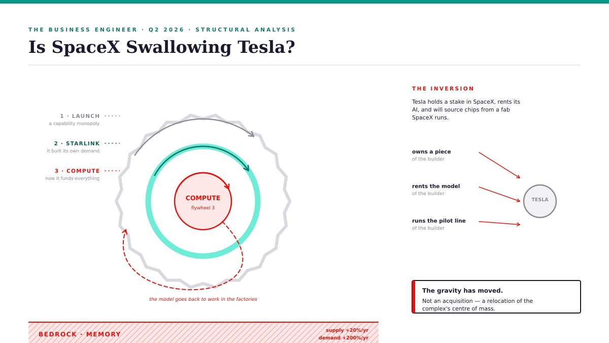
The more recognizable logic here is the SpaceX-conglomerate playbook applied to the silicon floor. SpaceX owns the rockets, the network, the models through xAI, and increasingly the data. The same instinct — that owning the entire physical stack beats renting specialized global suppliers — is now reaching for the fab itself. As we analyzed in our SpaceX conglomerate piece, the structural logic of the enterprise is consistent: vertical integration as a moat against suppliers, as a cost lever, and as a strategic hedge against dependencies that could become choke points at exactly the wrong moment.
The supply-wall framing is the most coherent reading of why this bet is being made now. Every major AI infrastructure builder — Microsoft, Google, Meta, Amazon — is confronting the same three bottlenecks simultaneously: TSMC leading-edge capacity, HBM memory allocation, and CoWoS/advanced packaging throughput. The standard response is to write larger checks to existing suppliers or to wait in longer queues. Terafab is the maximalist alternative: rather than negotiate for capacity, own the means of production end to end. Whether that beats the disaggregated supply chain’s efficiency is the multi-decade empirical question. That the bet is being made at all is the signal.
BE Framework — Vertical Integration to the Transistor
“The chip industry disaggregated because specialization at each layer was more efficient than integration. Terafab is a bet that in an era where compute is the strategic constraint, controlling the means of making it is worth more than the efficiency premium the disaggregated supply chain provides. That is a falsifiable thesis, not a certainty — and the funded first phase of $16.8 billion is a real but bounded commitment to finding out.”
Three Implications
IMPLICATION 1 — The Captive Fab Distinction Changes Everything
If Terafab is designed around SpaceX and Tesla’s own chip specifications — which may operate on less demanding process nodes than frontier AI accelerators — it is a sophisticated captive fab, not a TSMC competitor. That would be strategically coherent and genuinely achievable; it would also mean the announcement’s framing as a challenge to the global foundry order is significantly overstated. The node question is the one reporters have not yet answered, and it is the most important technical variable in the entire story.
IMPLICATION 2 — Execution Risk Is the Dominant Variable, Not Capital
The $16.8 billion first-phase check is real money, but capital is not the primary constraint here. No organization on Earth currently combines frontier logic process development, memory manufacturing, advanced packaging, and test at scale under one roof. The talent, tooling, and process expertise required to do all four simultaneously represent an execution challenge that has no modern precedent. Intel’s struggles over a decade of attempted vertical integration revival — at a fraction of this scope — are the closest data point, and they are not encouraging. The probability of partial failure on at least one of the four layers is high; the question is which layer and at what cost.
IMPLICATION 3 — The Signal Matters More Than the Outcome
Even if Terafab delivers only a fraction of its announced ambition, the strategic signal is durable: the most aggressive vertical integrator of the current era has concluded that the compute bottleneck is worth trying to own end to end, and has put a funded first phase behind that conclusion. That shifts how every other hyperscaler, sovereign fund, and national industrial policy must model its own chip dependency. The race beyond Nvidia’s moat is no longer only about software stacks and inference efficiency — it is increasingly about who controls the physical means of production.
Business Engineer Framework
The Map of AI Redrawn
Terafab is a bet being placed at the deepest layer of the AI stack — the physical semiconductor floor. The Map of AI framework maps 200+ companies across nine layers of the AI infrastructure and application stack, showing where value concentrates, where bottlenecks compound, and where vertical integration is a structural advantage versus an execution trap. Understanding where Terafab sits — and what it threatens — requires a working model of the full stack, not just the headline numbers.
Gennaro is the creator of FourWeekMBA, which reached about four million business people, comprising C-level executives, investors, analysts, product managers, and aspiring digital entrepreneurs in 2022 alone | He is also Director of Sales for a high-tech scaleup in the AI Industry | In 2012, Gennaro earned an International MBA with emphasis on Corporate Finance and Business Strategy.
Scroll to Top
Discover more from FourWeekMBA
Subscribe now to keep reading and get access to the full archive.